

PCB Panelization
PCB, or printed circuit boards, are the small green boards on which all the electronic components are placed within devices such as phones, televisions, and computers.
At Sunkey PCB,time-to-market and the economy are the key factors that we optimize for our customers in their favor. We do it in the most effective way, utilizing our experience and in collaboration with the customers at all stages Of electronic product design and manufacturing.
At the manufacturing stage, PCB Panelization is a clever method to produce many Of these boards simultaneously. Through this, we can streamline fab, assembly, and testing to process multiple PCB concurrently, leading to cost savings through reduced material wastage and time required for setup and teardowns. We will deep dive into this topic and cover it in two parts. Since manufacturing involves both the fabrication Of bare PCB and later assembling the components on these bare PCB so in part one, we will explain what panelization is, its types, when it is useful, different sizes Of the panels in use, and the important features Of the panel.
What is PCB Panelization?
If you have ever asked yourself how electronic gadgets are produced efficiently and in bulk, the solution very often involves the process of PCB panelization. To make it simpler, imagine you are baking cookies. Instead of baking one cookie at a time, you fill a tray with lots of cookies and bake them all at once. That's what panelization does, but with circuit boards! It puts many small PCB together into one big panel. That panel goes through the whole manufacturing process together, and later, the individual boards are snapped or cut apart.
Panel Types with respect to Manufacturing
In PCB manufacturing, there are mainly two types of panels.
Assembly Panel
Fabrication
Panel

In the manufacturing context, particularly in the production of PCB (Printed Circuit Board), a fabrication panel (or fab panel) is a master sheet with multiple individual PCB on it. The panel is employed to simplify the manufacturing process by enabling multiple boards to go through fabrication operations like etching, lamination, drilling, plating, and applying solder mask in batches. Fabrication panels usually have tooling holes for tooling and registration purposes, and different types of coupons. In the fabrication panel, individual PCB or assembly panels are placed in the X and Y axis 100-200mil away from each other, which allows for clean separation of the boards after fabrication is complete.
Fabrication panels are available in a variety of standard sizes to suit different production needs and PCB form factors. Common panel dimensions include 12 x 16 inches, 12 x 18 inches, 14 x 16 inches, 14 x 18 inches, 18 x 21 inches, 18 x 24 inches, and 21 x 24 inches, among others. Among these, the 18 x 24 inch panel is the most widely used size in the PCB fabrication industry due to its optimal balance of space utilization and compatibility with most production equipment. For applications that require larger PCB form factors, manufacturers also offer customized extended panel sizes, such as 21 x 32 inches, 30 x 30 inches, and even 30 x 40 inches. These extended sizes allow for high-volume production of large or complex boards, improving throughput and reducing material waste
Assembly Panel

This panel is designed for the automatic component placement and soldering phases. Assembly panels also have features such as tooling holes, strips known as rail area on the outside edges for conveyor handling, and fiducial marks for pick-and-place alignment. These panels can also provide spacing between boards to avoid component collision during assembly. A Fab panel can have multiple assembly panels during the fabrication process.
When to make an Assembly Panel?
In PCB (Printed Circuit Board) manufacturing at Sunkey, especially for SMT (Surface Mount Technology).assembly, we often need two straight, opposite edges on the PCB that are free of components. These clean edges are important for the machines to grip and move the boards smoothly.
We usually create an assembly panel (also called an array) when:
• The board has an irregular shape
If the PCB is not a simple rectangle or square, it's hard for the machines to handle it, so we put it in a regular-shaped panel.
• The PCB is smaller than 4x4 inches
PCB with a small form factor are difficult for machines to pick up and assemble,
so multiple small boards are grouped into a larger panel.
• The edge clearance is less than 200 mils
If components are placed too close to the PCB edges (where the machine grabs), we panelize to create safe gripping space.
• It's a mass production order
For big quantities, panels make the assembly faster and improve yield (fewer handling errors, better efficiency).

Features
of the Assembly Panel
An assembly panel, or an assembly array, refers to a custom designed setup of several PCB in an organized group for supporting automated assembly procedures like pick-and-place, soldering, inspection, and testing. These panels contain several structural and design aspects to promote efficiency, precision, and safety while assembling. Following are the most important features of an assembly panel.
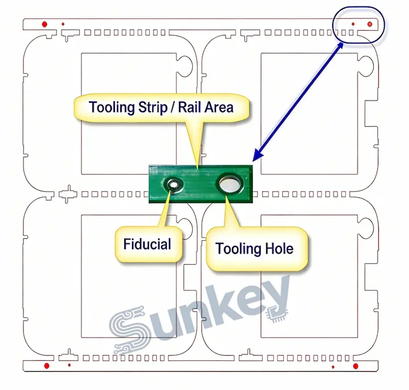
Tooling Strip/RaiI area
Tooling strips, or rails, are attached to the outer edges of the panel. These areas of no function are used to support conveyor systems, fixtures, or clamping mechanisms during assembly. They may feature fiducials and tooling holes that are used to align the panel accurately within assembly machines. The width of this trip varies from 200 mil to 400 mil depending upon the edge overhang component placements.
Fiducials
Fiducials are copper pads placed on the rails (border areas) of the PCB array. They serve as reference points for automated pick-and-place machines, helping the equipment accurately align and position components during assembly. Typically, fiducials are 40 mils in diameter and should be left uncovered by solder mask to ensure clear visibility for the assembly cameras.
Tooling
Holes![]()
Tooling holes are non-plated holes placed on the rails (border areas) of the PCB array. Their purpose is to secure the panel during assembly by allowing it to be pinned down, which helps prevent unwanted shifting or movement. The standard diameter for tooling holes is 118 mils (approximately 3 mm), but they can be drilled to custom sizes based on specific requirements.
we covered how panelization can save both time and material through the fabrication and assembly of multiple PCB in the panel at the same time. The higher the number of PCB we can accommodate in a panel (after consultation of Fab and the Assembly house), the higher are our gains in terms of both time and money. At SunKey, we utilize panelization as a tool to enhance the overall production efficiency by improving the quality and reliability of the final product. We start things keeping in view how we are going to end it. We essentially panelize multiple PCB into the panel, knowing that at the end, we have to separate them back to single PCB. This process is called De-Tabbing. In this article, we will be covering what de-tabbing is, what its different types are, how to define those in the panels, and how to select one in our panel.
How to separate the individual PCB from the panels?
Once the PCB panels are fabricated and components are assembled on them, the next important step is to separate the individual PCB from the panels. This process is called De-Tabbing. We will cover its details and types in Part 2.
De-tabbing Options
De-tabbing refers to the process of separating individual PCB from a panel after assembly. The method chosen depends on the board design, production volume, and edge quality requirements. Below are common de-tabbing options:
Route & retain with mouse bite holes
Route & retain with solid tabs
V-Scoring
Route & Retain with Mouse Bites (Perforated Tabs)

Small drill holes create a breakaway point, easy to snap off manually or with a fixture. After deburring, it leaves a slightly rough edge. If your PCB design has an irregular shape, tab routing may be required for panelization. For standard designs, we maintain a 2 mm (78.74 mil) spacing between adjacent boards in the panel to allow for proper routing and separation. However, if edge components (such as connectors) extend beyond the board outline, we must increase the spacing between boards to compensate for the overhang. For example, if an edge component extends 300 mil outside the board edge, we maintain a 400 mil distance between the two adjacent boards in an array. This additional spacing ensures easier de-tabbing and protects edge-mounted components during separation. Refer to the images below for examples of both standard and edge-component situations.
No Edge Overhang Components Edge Overhang Components![]()

Consider the following requirements when using route & retain with mouse bite hole depanelization method.

Key Points:
Avoid using on PCB thicker than 0.093' (2.3622mm)
Joint
strength using drilled breakaway routing is weaker than solid tab
routing
![]() Depanelization is by manual methods (hand, nibblers, plyers)
Depanelization is by manual methods (hand, nibblers, plyers)
Routed areas are smooth with some exposed fiber at tabs, leaving approx. +1-0.005' (0.1270mm) of material residue
Tabs should be positioned 0.078' away from edge components to avoid any damage to the component during de-tabbing
Route & Retain with Solid Tabs

In the Route and Retain with Solid Tabs method, the individual PCB are fully routed (cut) along their outlines, leaving solid tabs at certain points to hold the boards together within the panel during manufacturing and assembly. Since these tabs are unperforated hence provide greater panel strength during assembly, reducing flexing or warping.
Consider the following solid tab routing requirements when using the solid tab depanelization method.

Key Points:
The joint strength provided by solid tab routing is significantly higher than that of V-score or drilled breakaway (mouse bite) depanelization methods
Depanelization may only be performed with a machine, either a high speed automated router or shearing machine.
Routed areas are smooth, leaving < 0.005' (0.1270mm) of material residue. Tabs should be positioned 0.078' away from edge components to avoid any damage to the component during de-tabbing. It may involve part height considerations as well depending upon the type to tooling being used for the detabbing purpose.
V-Scoring

At SunKey,we also use V-Scoring (also called V-grooving) as a depanelization method where shallow grooves are cut into the top and bottom surfaces of the PCB along a straight line. These grooves are typically cut about one-third of the way through the board thickness on each side, leaving a thin web of material (about 1/3 thickness) that holds the boards together during assembly.
Consider the following requirements when using the v-groove depanelization method.
Parameter
Angle
PCB Thickness
Max Top to Bottom Misalignment
Web Thickness
Key Points
Specification
30 Degree
preferred for 0.062' to 0.093
0.004'
0.014' +1-0.002 '
Joint strength using V-score is weaker than solid tab routing and may be more susceptible to handling issues especially for larger panel sizes.
Depanelization may be performed manually or with a machine
Scoring provides a uniform but comparatively rough edge 0.004' to 0.010' Of residue material
If edge component placement allows, the boards may be placed adjacent to each other.
De-tabbing Equipment:
Even if your PCB array is designed well, problems can still happen when breaking the boards apart. If it's not done the right way, the board can splinter, tear, or damage components. That's why it's important to use proper de-tabbing methods and tools to avoid extra costs.
Pliers & Nibblers
A well-designed tab-routed PCB panel can often be broken apart using hand tools. For best results, use wide-nose pliers to bend each tab along the break line until you hear it crack. Then, bend the tabs the other way to completely separate the boards. This de-tabbing method can be used mostly for the tabs having mouse bite holes.

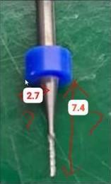
Second Route Operation
Another way to separate PCB from rails or each other is by using a high-speed routing machine. As shown in the picture below, this method uses a router bit and requires careful attention to the size of nearby components. If a part is placed close to a solid tab, its height and width must not exceed 7.4 mm and 2.4 mm. Otherwise, the secondary routing process could damage the part. We carefully take all Of these factors into account when designing array drawings.
Pizza Type Auto/Manual PCB Cutter
This method uses a newly designed linear or circular cutter that completes the micro shearstress cutting stroke in a single motion. It's suitable for all types of tabs. During the process, the PCB remains stationary while the cutting blade moves back and forth. This helps minimize shear stress and reduces the risk of product quality issues. The cutting machine is made of highspeed steel, making it durable and reusable


 :
: :
: : A1 Building,Ditang Industrail B zone,Shajing Street,Bao'an
  :+86 13244860273

